
GPIO Test 1
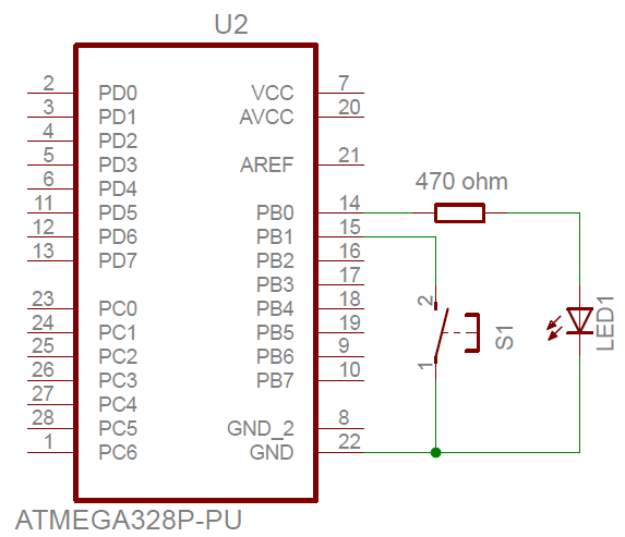
Connection Diagram
Functions
LED1 at PB0 turns ON when the Switch S1 at PB1 is closed.
LED1 at PB0 turns OFF when the Switch S1 at PB1 is open.
gpio_test_1.c
#include <mega328p.h>

void main(void)
{
    // Port B initialization
    // Func7=In Func6=In Func5=In Func4=In Func3=In Func2=In Func1=In Func0=Out
    // State7=T State6=T State5=T State4=T State3=T State2=T State1=P State0=0
    PORTB = 0b00000010;    // enable pull-up at PB1. Refer to the 3rd paragraph of <14.2.1 Configuring the Pin>
    DDRB  = 0b00000001;    // set PB0 as output

    while (1)
    {
        if ((PINB & 0b00000010) != 0)       // SW is open
            PORTB &= ~0b00000001;           // LED off. Same as PORTB &= 0b11111110
        else
            PORTB |= 0b00000001;            // LED on

    }
}
The voltage across PB1 and GND is the same as VCC when the switch S1 is open and this voltage (VCC) is considered as logic HIGH level inside of ATmega328P microcontroller.
On the other hand, the voltage across PB1 and GND is 0 V when the switch S1 is closed and this voltage (0 V) is considered as logic LOW level inside of the microcontroller.
In C language program, the logic HIGH level is expressed in binary number one (1) and the logic LOW level is expressed in binary number zero (0).
The voltage level at PB1 can be evaluated by reading PINB register. The binary value of bit 1 of PINB register will be one (1) when the switch S1 is open and it will be zero (0) when the switch (S1) is closed.
PORTB &= ~0b00000001;
In C language the tilde symbol (~) is an operator taking one's complement of the number followed. Therefore, the above program line has the same meaning as following.
PORTB &= 0b11111110;
In addition, the &= is an operator taking bitwise AND and assignment. So it can be expanded as following.
PORTB = PORTB & 0b11111110;